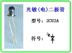
Photodiodes, also known as photodiode, which is a photoelectric conversion semiconductor devices, photosensitive resistor compared with the high sensitivity, good high-frequency performance, reliability, small size, ease of use.

Figure 1 Photodiode
1. Structural features and symbols
Photodiode and ordinary diode although both belong to the one-way conductivity compared to non-linear semiconductor devices, but the structure has its own special place.
Photodiode symbol in the circuit shown in FIG. Photodiode when used to reverse the access circuit, ie positive then negative power supply, negative positive power supply.
2. Photoelectric conversion principle
According to the PN junction reverse characteristic found that within a certain range of reverse voltage, the reverse current is small and in a saturated state. In this case, if the light irradiation PN junction, due to the intrinsic excitation of electrons - hole on a limited number of reverse saturation current remains unchanged, in the photosensitive diodes called dark current. PN junction when light is irradiated, it will produce a large number of nodal additional electron-hole pairs (called photo-generated carriers flowing through the PN junction current increases light intensity and surge, this time back Current known photocurrent light of different wavelengths (blue light, red light, infrared light) in different regions of the photodiode is formed the light is absorbed current is absorbed by the surface of the P-type diffusion layer is mainly shorter wavelength blue light, In this area, due to the light produced by the light-generated carriers (electrons) Once the drift to the depletion layer interface, will be in action at the junction electric field, pulled to the N region formed part of the photocurrent; longer wavelength red light, The excited electrons in the depletion layer through the P-type layer - hole pairs, these new electron and hole carriers will be under the electric field at the junction, respectively, to reach the N and P region to form a photocurrent wavelength more. Long infrared light transmitted through the P-type layer and the depletion layer is directly absorbed by N zone. In the N region due to light produced by the light-generated carriers (holes) drift to the depletion region once the interface, will be in the junction field It is pulled under the action of the P region to form a photocurrent. Thus, when irradiated with light, the light flowing through the PN junction current should be the sum of three parts photocurrent.


